This page contains a "relatively free" translation by DrCoolZic of the original article, published in the French ST Magazine N°44 September 1990, about the Atari STE Hardware. You can find a French online version of this article here.
Note for the French reader: The original writting uses an extremely circonvoluted style with sentences that span over many many lines and usually contain many distinctive information. I did lots of "cleanup" and therefore I beleive that my translated text is easier to understand (as long as you read English!).
Atari STE Motherboard Presentation
The following picture of an Atari 520 STE motherboard is taken from the HxC2001 site:
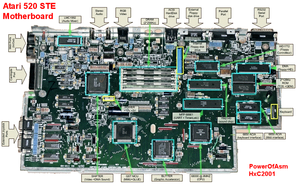
The Main Components on the motherboard:
- 68000 (Motorola) 8Mhz Processor
- 68901 (Motorola) Multifunction Peripheral. Used mainly to manage interrupts, for the Timers and serial ports
- Blitter (Atari): Graphical component allowing to display sprites in HW.
- GST MCU == Glue + MMU (Atari): Contains most of the internal Atari glue logic, DRAM Management, Clocks generation, Address decoding, and the New joysticks/paddles/pen manangement.
- GST Shifter (Atari): Video management component, contains also the sound DMA.
- DRAM : SIMM modules. On the original 520STE 2 x 256Ko modules
- YM2149 (Yamaha) : ST Sound component
- 6850 (Motorola / ST) : Serial controller used for the MIDI and Keyboard interfaces.
- ROMs (256KB) contains the TOS (1.6) and the GEM.
- DMA controller (Atari): for the Hard Disks and the Floppy Disks
- WD1772 (Western Digital) : Floppy Disk Controller
- LMC1992 (Nationnal) : Sound mixer. Used to adjust the sound characteristics (Ballance, Trebble, Bass, ...)
The Atari STE Hardware
The release of the Atari STE has opened many questions like "what are the performances of this new machine". The great programming capabilities of the STE have been discussed in many places but, until now, no thorough study of the hardware was made (that also includes the changes compared to the STF range). This article is particularly dedicated to the "Hardware gurus", but also to the curious programmers, wishing to better understand the STE machine.
The literature on the hardware of the STF and the STE is relatively poor. Therefore in order to be understood by everyone I have tried to be as complete as possible, using also references to the preceding STF range.
During operation, all the circuits of an ST machine works very tightly together. It is therefore not easy to split the hardware into distinct sections, such as sound or video. Although, to facilitate the life of the programmers, the addresses of the registers used by the different components have been grouped in zones corresponding to specific functions, the actual physical location of these registers is often dispatched on several circuits. It is therefore good to start this study by looking at the pinout of the main components of an STE.
As they implements various functions in the STE be prepare to make a lot of jumps in the text while reading!
Note-1: To speak about the old range, I will reference it as the STF which obviously also includes the MEGA ST.
Note-2: The following convention is used for the pins and signals -- if a name is preceded with a star the pin or signal is active low.
Back to the topThe Glue and MMU of the STF
During the design of the first ST, the Atari firm has designed two large ASIC known under the name of the MMU and the GLUE. These two components integrated all the TTL circuits that could be found on the five large prototype boards created by the end of 84.
The GLUE, as its name indicates, ensures the cohesion of the STF system and is responsible for the following tasks:
- decoding of the address in the 16MB zone accessed by the 68000 for selection of the circuits using the data and address buses,
- generation of a bus error signal (resultsing in the well known two bombs) if you address an invalid area or if you address an area requiring the 68000 "supervisor mode" while in "user mode",
- delivery of the video synchronization signals,
- management of the interrupts coming from the 68901 (MFP),
- management of the hardware priorities on the bus, as well as the arbritation of the bus.
The MMU (Memory Management Unit) ensures the management of the RAM memory. The MMU is also the main circuit for the address management of the video RAM (used for the scrollings), as well as the follow-up of the discs transfers done by the DMA circuit. But we will see that in detail later…
Back to the topThe GST MCU
 As finer scrolling capabilities were targeted for the new machine, the MMU had to be completely re-examined. Also, in order to use less room and to reduce the number of tracks on the boards, the MMU has been merged into the same package with what should have been the successor of the GLUE.
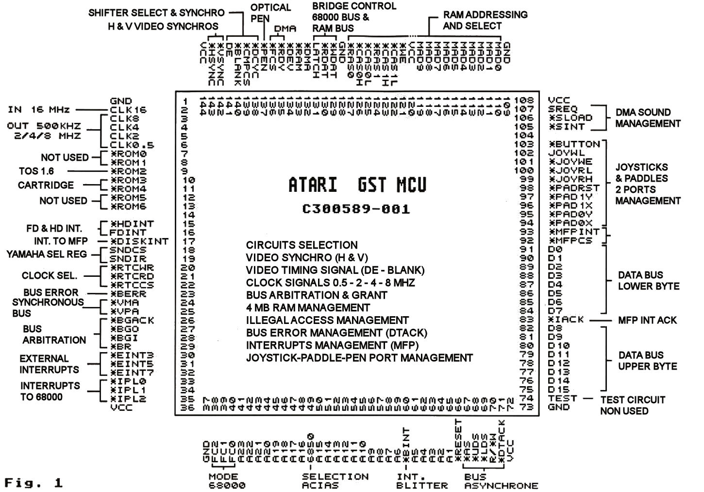
This new component takes the name of GST MCU (Memory Controller Units). It is an impressive CMS package with 144 pins. This does not leave any chance of repair to whoever does not have the necessary material to solder this "monster"…
The pinout of the GST MCU is shown in figure 1. In addition to the GLUE and the MMU functions, it is also in charge of the address management for the 8 bits stereophonic sound transfered through a DMA, as well as the management of two new joysticks and paddles ports, plus an optical pen.
As the address bus of the GST MCU is now 23 bits wide, it allows decoding of addresses in a 16 MB zone of the 68000. Therefore it could have been possible to manage more than 4 MB of RAM, as this limitation in the STF was due to the usage of a 21 bits address bus in the MMU. But unfortunately, there are still the same number of multiplexed address pins for the RAM circuits (MAD0 to MAD9), and there is no additional selection pin for new banks of RAMs. Therefore this implies that the STE is still limited to 4 MB of RAM!
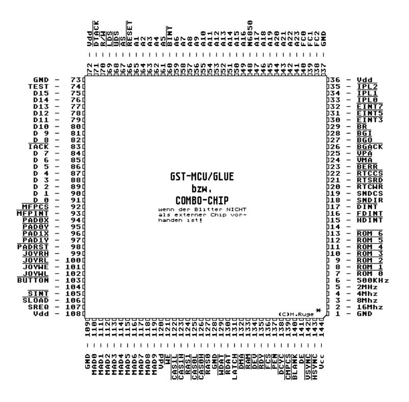
IMPORTANT: The pinout shown above is incorrect. Pin 48 and 49 should be swapped as well as pin 18 and 19. Therefore we have pin 18=SNDIR, pin 19=SNDCS, pin 48=N6850, pin 49=A16 (for an updated picture with the correct pinout click here). Many thanks to David S. for testing on an STE and reporting the error. I leave the picture with the wrong pinout for reference as it provides some nice information.
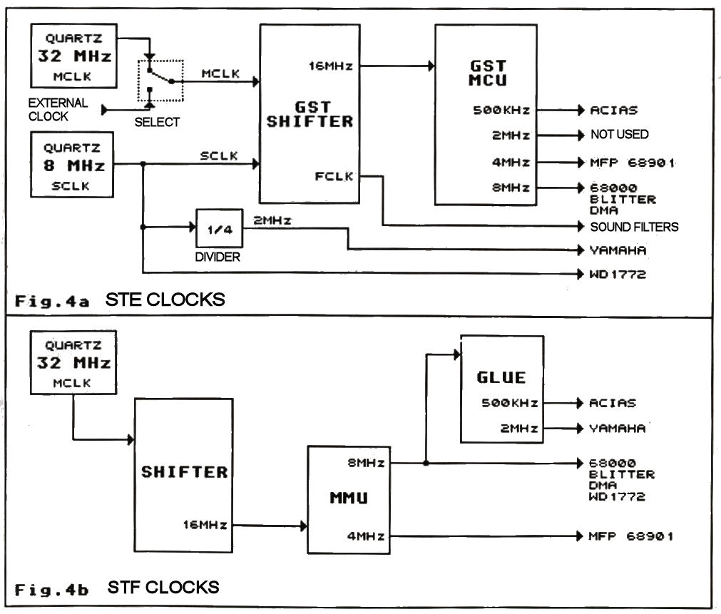 Pins 2 to 6 are the input and the outputs of the different clocks used by various circuits on the motheboard. The 16 MHz input comes, as before, from the video circuit (GST Shifter). The following output frequencies are available from the GST MCU: 0.5 MHz, 2 MHz, 4 MHz, and 8 MHz. For their usage, refer to figure 4 which presents the clocks distribution of the STF and the STE.
In the STF, the AClAS (6850 managing the keyboard serial connections and the MIDI) receive a 0.5 MHz clock, the old sound circuit (Yamaha YM-2149) a 2 MHz clock, the MFP (68901 used for interrupts and the RS232) a 4 MHz clock, the 68000, the Blitter, the DMA, the WD1772 (FD controller) and the GLUE a 8 MHz clock, and the MMU a 16 MHz clock.
The new GST MCU provides all the frequencies previously delivered by the GLUE and the MMU. However the new shifter (GST SHIFTER see figure 2) receives an 8MHz clock coming from a separate oscillator. This clock called SCLK (Sound Clock) allows, via some internal dividers of the GST Shifter, to generate a clock with an ajustable frequency (FCLK). This clock is used for the sound filters which we will talk about a little bit further. The signal of this oscillator is also used by the WD1772 and divided by 4 to obtain a frequency of 2 MHz used by the Yamaha YM-2149.
You may have noticed that the 2 MHz output of GST MCU is not used, though completely functional (I have checked this by connecting the YM-2149 to it)… In fact, the new 8 MHz oscillator is intended to provide a stable clock to all the circuits which could have synchronization problems if the basic 32 MHz video clock is changed. This happen when the machine is switched from the internal 32 MHz oscillator to an external oscillator that has roughly the same frequency (for example 36 MHz). Switching to this external clock is necessary in order to synchronize the internal video source of the ST with an external source. This allows to mix the two video signals for incrustation of one on the other: genlock function. The Genlock (for generator lock) is a common technique where the video output of one source, or a specific reference signal, is used to synchronize other sources together. With the example of a 36 MHz external frequency, the GST MCU would not provide any more a 8 MHz frequency output but 9 MHz. This would cause problems for the WD1772 that would not recognize correctly floppy discs formated on a normal ST operating with a 32 MHz clock. A similar problem would happen for the DMA sound managed by the GST Shifter as we will see it. As for the YM-2149, it would not receive a 2 MHz frequency from the GST MCU, but of a 2.25 MHz (9/4), which would make it play false! I have been able to check that this 8 MHz oscillator does not have any utility in the case of an ST running under normal condition, by replacing it by the CLK8 clock of GST MCU. Note that the SCLK entry of the shifter is only necessary for the management of the sound DMA. I have disconnected the SCLK clock and the STE was still working perfectly well, with the exception of the sound that had disappeared.
 Then comes the *ROMx pins used to select the ROMs of the STE. Each signal is activated when the processor access a certain area of the memory (this is called address decoding).
In my study, I have discovered several areas -- corresponding to the signals *ROM0, *ROM1, *ROM5 and *ROM6 -- which are currently not used (see figure 13 for the exact addresses). The discovery of these 256 KB address areas is very interesting. It allows, for example, to have programs running in Eproms at these addresses…
The signals *ROM4 and *ROM3, as on the STF, correspond to the usage of the cartridge port in the areas respectively of $FA0000 to $FAFFFF and $FB0000 to $FBFFFF.
The *ROM2 signal is used on the STE to select the 2 x 128 KB roms containing the TOS 1.6. On the STF, this signal was combined with the *ROM0 and *ROM1 signals to allow addressing of three zones of 64 KB corresponding to three pairs of 32 KB roms used by the TOS 1.0 and via a three inputs AND gate, to a pair of 128 KB roms for the TOS 1.2 (blitter).
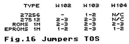
The two ROM sockets used by the the TOS 1.6 have 32 pins. The first STEs were equipped with 2 x 1 Mbits 32 pins Eproms, whereas they now uses 28 pins Roms which are installed in these two sockets.
Therefore you will find on the STE board three small jumpers -- referenced as W102, W103 and W104 -- which allow to ajust the signal connected to pins 2, 3, and 24 of the two sockets depending on the type of ROM used. You will find all the possible configurations of these jumpers on figure 16.
 While we are talking about ROMs, I must tell you that we have disassembled the beginning of Roms and we have seen that this new TOS 1.6 tests for the possible presence of a 68030! This is done by testing the bit 9 of the CACR (Cache Address Control Register), the result being put into a new sytem variable. In the case of the presence of a 68030 some routines using faster instructions specific to the 68030 are used.
Moreover the two large incompatibilities which prevented the 020 and 030 to function have been corrected. These two incompatibilities are: the usage of Line F, and some instructions which refuse to be executed in 'user' mode on the 020 and 030. First, the Line F does not seem to be used any more by the 68000, and is replaced by several TRAPs. Second, a 'priviledge violation' routine has been installed to catch the error occurring when the 030 operate in 'user' mode for an instruction which is now only usable in 'supervisor mode'. But currently this routine has some bugs that prevents it from running! Perhaps we will have the occasion to present some "patches" for this TOS. This imply that it should be possible, when the bugs will be corrected, to use a 68030 (from a software point of view) with this TOS. In fact, this TOS seems to be a pre-version of the TOS 030 which will be used by the TT.
Note that a 68020 will be recognized like a 68000, and therefore will not benefit from specific routines, as the bit 9 of the CACR does not exist in the equivalent register of the 68020 (4 bits only).
Next we find the *HDINT and FDINT interrupt signal inputs that takes the signals coming respectively from the hard disk controller (HD) and from the floppy disk controller (FD). These two signals do not go to the MMU of the STF, and this is a considerable difference. For better understanding the huge software improvement which results from this, it should be known that until now the I05 interrupt pin of the MFP is not activated (including on the STE) for an unknown reason. Therefore on the STF a DMA disk transfer requires a software polling (DMA routine) throughout the operation to monitor the DMA counter. The MMU cannot know by itself when it must stop incrementing its DMA counter because there is no DMA end of transfer register as it is the case for example with the sound DMA transfers of the STE as we will see later. Obviously this routine uses time from the system. It must indeed compare the incremented value with the number of data to be transferred throughout the transfer, then when the two values are the same, to desactivate the DMA mode in the MMU. In the STE, the GST MCU receives now an interrupt signal indicating the end of a DMA disk transfer and thus knows that it must stop incrementing the counter and addressing the RAM. Therefore the hardware management is simplified and thus faster. The signal *DISKINT is the signal resulting from a logical NOR operation on *HDINT and FDINT and is directed on the I05 interrupt pin of the MFP.
The pin 19 (SNDIR) allows to specify the registers of the YM-2149, and the pin 18 SNDCS (SouND Chip Select) selects the YM2149 following an address considered by GST MCU as being one of those used for the YM2149.
Three following pins (20 to 22 *RTCWR = Real Time Clock Write, *RTCRD = RTC ReaD; *RTCCS = RTC Chip Select) are intended for the management of a battery backup clock circuit. These three pins are the same as those present on Mega ST for the clock circuit. In the Mega ST they come from a PAL (programmable logical circuit) to perform the proper addresses decoding required for the management of the RP5C15 clock circuit (zone of address of FFFC20 to FFFC3F). It was thus normal to benefit from the integration of GST MCU to also add the decoding of this zone, but why not have put this clock circuit on the board?!
On pin 23 we find the BERR (Bus Error) signal sent towards the 68000 to indicate an attempt to read or write in a protected or prohibited area. But the BERR can also be sent when the DTACK signal (data transmition acknowledge) will not be emitted by the peripheral, because the data did not arrive to it or where not sent back to 68000. In those cases, the GST MCU acts as a "watchdog" : it waits for a certain period, before estimating that it is necessary to give up and announce the problem to the processor. You have to know that as long as the 68000 did not receive a DTACK or BERR signal, it loops into a wait state mode. This process is often used on machines where the processor must wait to access slow RAM.
The two following signals are used for synchronous bus communication between the processor and slow peripheral circuits of the 6800 family such as the ACIAS 6850. For this type of communication, a synchronization clock signal called E (Enable or 02 in the 8 bits processors jargon) is emitted by the 68000. It has a frequency of a tenth of the processor, that is to say here 800 Khz. The VPA signal (Valid Penpheral Address) is sent by GST MCU to the 68000, to inform it that the address that has just been placed on the bus is an address corresponding to a circuit of the 6800 family (address decoded by the GST MCU). In this case, the processor waits for the E signal to go low, then it sends the *VMA signal (Valid Memory Address), to inform the GST MCU that it is synchronized with the signal E and that the address presented is valid. The signal *VMA can be regarded as a selection signal of the peripheral circuits even if in the case of a ST an ACIAs (6850CS) selection signal is generated from the *VMA signal. The Signal VPA is also used to indicate to the processor an auto-interruption (auto-vectors 25 to 31).
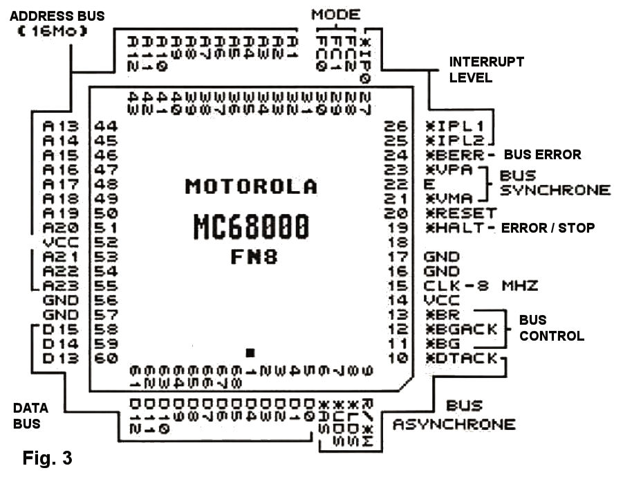 Pins 26 to 29 are the bus arbitration signals: we find the traditional BR, BG, and BGACK also present on the processor (see figure 3 for the pinouts of the 68000). BR is emitted towards the 68000 to indicate that a circuit request to become the 'busmaster' (owner of the bus). This circuit can be the Blitter or GST MCU (for the DMA). In fact, the Blitter has also these signals and thus does not need the GST MCU to make the request to the 68000 (see ST Mag n° 26 about the Hardware of the Blitter), but the GST MCU has also a role to arbitrate and avoid congestions on the bus. The DMA circuit is obliged to send a signal to request the bus (*RDY) to GST MCU. At this time, the GST MCU sends a *BR (Bus Request) to the processor which finishes its bus cycle in progress before sending a signal *BG (Bus Grant) to inform GST MCU that it now has the bus allotted. It then sends a *BGACK (Bus Grant ACKnowledge) to the processor to inform it that it takes the responsibility of the bus, and this until this signal is return to a high level, at this moment the processor takes again ownership of the bus. When the bus is used by the Blitter or the DMA, practically all the pins of the 68000 processor are set to an high impedance state. The pin *BGO is an output of the signal *BG, originally used by the bus connectors of Mega ST, it is therefore not used in the STE.
The same apply to the interrupt input pins INT3, INT5, and INT7. With these pins, you must associate the INT6, INT4, and INT2 used on all the ST systems. On Mega ST, a priority encoding circuit (74LS148) receives the INTx pins and sends a signal coded on 3 bits to the three *IPL pins (Interrupt Priority Level) of the 68000, to indicate the level of the received INT (see the article “Bus stop” ST Mag n° 30). Of course, the pins INT2, INT4, and INT6 were never visible since in fact they are managed by the GST MCU to indicate respectively HBL, VBL, and MFP interruptions. The 74LS148 circuit has also been integrated into the GST MCU and its three output pins *IPL0, *IPL1, and *IPL2 are directly connected to the corresponding signals of the 68000 (see fig. 3).
The three FC pins (Function Codes) are connected to the corresponding pins of the 68000. This allow to indicate to the GST MCU in which mode it works (user, supervisor or detection of interruption -- which can be caused by certain opcodes like those of the line F), in order to help the detection of illegal addressing.
The Pin 60 *BINT is the interrupt sent by the Blitter, which is new, since until now only the MFP received this signal which was not taken into account by the system. I have not been able to determine the role of this signal for the GST MCU because contrary to a DMA disc access, for which GST MCU takes in charge the bus and must thus know when to release it (*HDINT and FDINT signals), the blitter does not go through the GST MCU to take and return the bus. Moreover, based on the configuration of the MFP, it seems that this signal is still not taken into account on I03 pin. The *RESET signal is necessary to GST MCU to reinitialize its internal counters (video, DMA, etc).
The five following signals are the traditional signals used for asynchronous bus exchange. The four first are emitted by the 68000. R/*W indicates to the peripheral if the processor wishes to read or to write a data. *UDS (Upper Data Strobe) and *LDS (Lower Data Strobe) indicate respectively if the 68000 works out of the 8 upper or lower bits of the bus, but if the processor works with words (16 bits) or long words (32 bits), then these two signals are activated. The signal *AS (Address Strobe) is activated just after the address was placed on the adress bus by the 68000, to inform the peripheral that the presented address is valid. As for the signal *DTACK (already describe above), it is sent by the peripheral to announce to the 68000, either that the data on the bus are valid in the event of reading by the 68000, or that the data were received in the event of writing. In both cases. it indicates to the 68000 the end of a transfer cycle on the bus.
Pins 83,92 and 93 are used for the management of the MFP. On the pin *MFPINT, the MFP informs GST MCU that one of the sixteen interrupts has just been started, either internal to the MFP, or one comming from the eight bits of its port. The GST MCU, once the 68000 is informed and that the MFP announces that it is in interrupt mode by its three FC pins, sends an interrupt acknowledge (*IACK = Interrupt ACKnowledge) to the MFP to let it know that it can send the interrupt code on the lower 8 bits of the data bus to the processor. The pin *MFPCS is used to select the circuit when the 68000 wants to read or write one of its the registers.
The group of pins 94 to 103 are used for the management of the two new joysticks/paddles/optical-pen ports which we will see towards the end of this article. Same for the pins SREQ, *SLOAD and *SINT which are connected to the shifter for the management of the new sound in DMA.
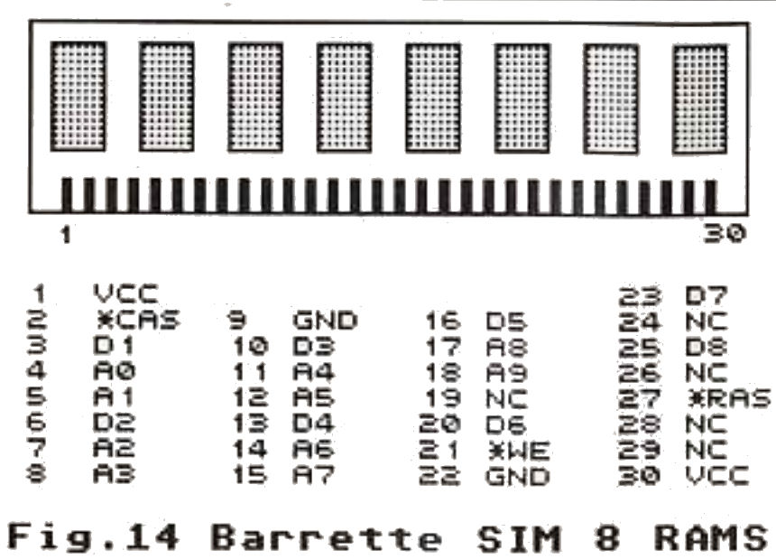 On Pins 110 to 127, we find the signals of the multiplexed adress bus and those for the selection of the two RAM banks -- with a maximum of 2 MB for each one. The STE can accomodate up to to 4 MB without any soldering, since the motherboard is equipped with four sockets intended to receive SIMMs (Single Inline Memory Modules) or SIP (Single Inline Package) modules of 256 KB or 1 MB. You will find the pinout of these modules on figure 14. It should be noted that the management of the memory by the system has been modified, since a 2.5 MB memory configuration -- with two 1 MB and two 256 KB modules -- is not recognized any more by the system. Note also that the diagnostic cartridges of the system reports 2 MB of RAM for machines with 512 KB! This is strange as an inspection of the MMU configuration register has enabled me to check that the values allotted to various RAM configurations were always the same ones. It is thus impossible for me to give an explanation, but the 3 seconds latency of the STE at startup could be due to a twisted management of the RAM. One can think that a routine to test the RAM at the boot time is launched by the TOS 1.6 and that it is not able to recognize a 2.5 MB configuration.
Then we find three signals which were before sent by MMU to control four TTL circuits (LS244 and LS373). These circuits are used to connect the Shifter and Rams data bus with the 68000 data bus. The four TTL have now been integrated in the shifter.The signals *DMA, *RAM and *DEV are not used outside of the GST MCU, but are on the STF, sent by the GLUE for the MMU. The *DMA allow to select the DMA count registers of the MMU for a DMA disc transfer. The *RAM indicates that an access to the RAM is detected by a decoding the address of the GLUE (zone of $000008 to $3FFFFF = 4 Mo). Following the reception of this signal, the MMU activates the TTL 244 or 373 circuits depending on the direction of the data transfer as indicated by the signal R*W. As for *DEV, it allows to select the counters of the video registers (VBASE and VCOUNT) to address the video RAM bound to the shifter and perhaps also the internal registers of the shifter (colors and resolutions) via signal CMPCS, if this last is not decoded in the MMU. The signal *FCS is sent towards the DMA to select its registers (access to the WD1772 and status of the DMA).
If the circuit needs the data bus to send or receive a word, it sends the *RDY signal to the GST MCU which in turn request release of the bus (sending of a *BR to the 68000). It should be noted that the data bus of the DMA connector is buffered with a 74LS245. The direction of the data is controled by the signal CR/*W sent by the DMA circuit. The buffers validation of this circuit is carried out by the signal *FDCS (Floppy Disk Chip Select) sent by the DMA circuit towards the WD1772 via a flip-flop (74LS74) receiving the CLK8 clock. Thus, when the WD1772 is selected, the DMA bus is isolated from the connected peripheral. This bufferization will avoid to damage the DMA circuit if a connection is done when the system is running. The control signals, namely R/*W, A0 *HDACK (Hard Disk ACK-nowledge), and RESET, are buffered by a 74LS244. It is one of the buffers of this circuit which drives the signal *DSO (Drive Select 0) bound for the orange led. The signal *PEN (137) is used by the optical pen connected on the new port 0 (DB15).
 The four following signals are sent towards the GST Shifter to synchronize it with the data transfer of the video RAM as well as the signals VSYNC and HSYNC which were generated by the GLUE in the STF. *DCYC (Data CYCIe) indicates to Shifter that the data are available from the RAMs (i.e. the GST MCU has just selected the RAM address of the next data to be loaded in the GST Shifter; this addressing is carried out 16000 times per image in connection with the VCOUNT counters of GST MCU (or of the MMU in a STF). DE (DisplayEnable -- active at the high level) indicates to the video circuit that it must send a line of video to the monitor. This signal is active during the sending of each line in direct relationship with signals VSYNC HSYNC, it is for this reason sent by the GLUE of the STF towards the Shifter, but also to the MMU of STF. Lastly, DE is also received by the MFP on the input of its timer B (recognized on the falling edge, i.e. at the end of the display of the line) so much used for the video effects.*BLANK is sent at the end of each image to avoid the transmission of video signals outside of the screen display zone, time it takes to the video gun to get back to the top left corner of the tube. In the same way DE is in relation to signals VSYNC HSYNC and is thus sent by the GLUE of STF. The signal *CMPCS selects the Shifter for the access to its registers. The configuration register for synchro (50/60 Hz and synchro int. /ext.) is in GST MCU (and GLUE of the STF) and not in the Shifter, as the localization of the address of this register (see figure 10) could let it think . It is for this register that the GLUE of the STF is provided with two data pins connected to bits 8 and 9 of the bus, which corresponds well to the 2 modifiable bits of the register. But if that explains how the GLUE knows if it must send 50 or 60 Hz synchros, how does it knows that it must send 71 Hz (high-resolution)?
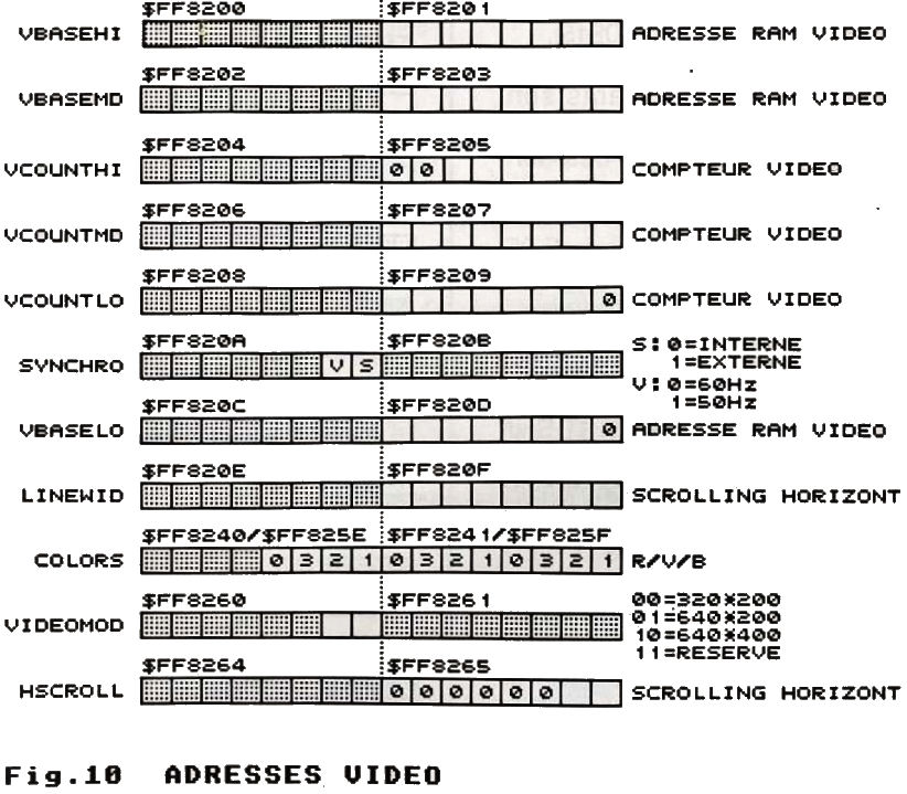
In fact, if you look at the video addresses (figure 10), you will notice that another register is also on bits 8 and 9: VIDEOMOD which makes it possible to indicate the resolution to the shifter, but also to the GLUE (GST MCU on STE). Thus at address FF8260 correspond two registers one in the shifter and one in the GLUE. The only video registers which are in the shifter of the STF are the COLORS and VIDEOMOD. Indeed, this shifter only has 5 bits of address. The GST SHIFTER is equipped with a sixth address bit address for the additional register HSCROLL and certain registers of its sound DMA, but all the other video registers of figure 10 are in located in the GST MCU.
Back to the topThe GST Shifter
 The new video circuit of the STE (see figure 2) is more powerful than that of the STF and, in addition to its extended graphic possibilities, it ensures also the management of the DMA sound, the great innovation of the machine. Above all, two notes: I could not find the function of the pin 73 (LOWP) which is not used. Then, pin 51 (COLOR) is unfortunately not a composite video out, but a video color clock signal (NTSC) used by the video composite modulation stage (only for the PAL/NTSC models equipped with an output RF antenna). It is completely possible to obtain a composite video (to send to a video tape recorder) by adding the components of the first stage, and also those of the section charged to create a frequency for the color clock, then exploited by the composite video stage built with a RVB PAL/NTSC encoder.
The GST Shifter is equipped with two 16 bits data buses: one is connected on the machine (68000) data bus, and the other is connected directly to the RAM (1 bit by RAM of each bank). On the preceding models, the link between the two buses was made by four TTL circuits which were controlled, as we have described above, by the signals LATCH, *RDAT, and *WDAT emitted by the MMU. In fact nothing has changed, but the circuits are now in the Shifter. The insulation of the two buses is one of the strong points of ST. Indeed when the Shifter needs to reach the RAM, the insulation is effective, and during this time the 68000 still has access to its data bus and can work with peripheral circuits. In the event of a need to access the RAM, the two buses are connected together by the MMU which avoids to do this while the Shifter performs a RAM read cycle (400 000 times per second!). In fact, the Shifter reaches the RAM like a DMA circuit without passing by the processor.
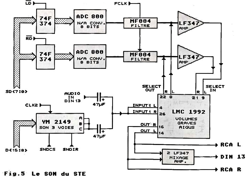 It is on this principle that the new sound is managed. For that, the Shifter has a third data bus, of only 8 bits (SDO with SD7), which transports the data of the Shifter towards the two digital/analog 8 bits converters as you can see on figure 5. But before commenting on the sound circuitery, let us return to the principle of its DMA managed by the Shifter. As for the disc DMA, the counters of the sound DMA (see addresses figure 11) are located in the GST MCU, and thus the Shifter has the SREQ (Sound REQuest) and *SLOAD (Sound LOAD) control signals. This last is the counterpart of *LOAD used for the video. It is emitted by the GST MCU to indicate to the Shifter that the address of a data (16 bits) in RAM is present, and that the data at this address are available on the RAMs bus. At this time, the shifter reads the word and then sends it in a succession of two bytes on the bus connected to the two converters. But so that each converter receives the good byte, each one is connected through a 74F374 (eight bits flip-flop) which transmits its 8 bits at reception of a signal (*LD and *RD) transmitted obviously by Shifter (pins 19 and 20).
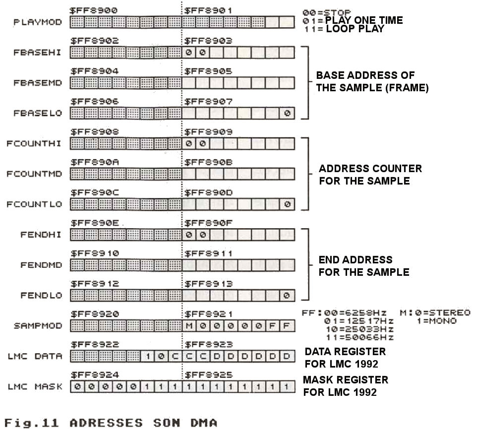 The signal SREQ is sent by the Shifter to the GST MCU to request it to address a word in RAM. This signal precedes the *SLOAD. The access frequencies (frequencies of sending a word towards the converters) are 6258 Hz, 12517 Hz, 25033 Hz, or 50066 Hz. When the access to the sample finishes (sound counter), the GST MCU sends an interrupt signal *SINT on the pin I07 of the MFP (a level 7 interrupt, equal to the one of monochromic detection), but also on TAI pin of the MFP (Timer A Input) which was connected on the STF to pin 10 (input of the signal busy from the printer) without much interest.
In fact, it should be known that if the first series of the STE boards were indeed connected according to the above description, a component, (those who have opened the machine must have noticed it) has been added with some extra wires. This component is a 74LS164, a 8 bits counter, which intercepts the *SINT signal which was sent originnaly on the input of the timer A in order to delay it before sending the result on this same timer (see figure 15). We carried out some software tests, and the function of this timer is not obvious. According to the frequency of the 2 MHz clock received and the output of bit 8, one can estimate that the time, between arrived of a signal on A and B and the output on bit 8, is of 8 x (1/2000000) = 4 microseconds.
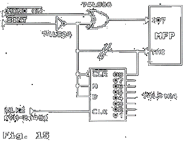 If the signal *SINT is not active (high level) the counter has its *CLR pin at the low level, as well as the output bits. At the end of a sample, the GST MCU places the *SINT at a low level and pins A, B, and *CLR are at the high level, which means that the counter is active and is incremented with each clock pulse. 4 microseconds later the output 8 of the counter is at the high level, and the change of the MFP input (TAI) from the low level to the high level increments the counter of the MFP. Of course, it is necessary that the signal *SINT lasts more than 4 microseconds, if not the counter will be reset to 0 before it have reached its output on bit 8 and the MFP will not receive any change of state.
Thus the role of the added circuit seem to only delay the arrival of the interrupt signal to the timer. But the end of sample interrupt is also sent on the highest interrupt (I07) pin through an XOR (exclusive OR) gate with the monochrome detection.
Two cases can then arise:
- we are in color mode and thus the signal *MONOON is at the high level. If there is no interrupt, there is one 1 on I07, but in the event of arrival of an interrupt, the output of the XOR gate passes to 0 and this transition in a low state announces to the MFP an interrupt. The result is the same if a monochrome screen is connected a transition to low level of *MONOON. You will notice that for the hardware, it is impossible to know if the monochrome screen has just been connected or if it is the end of a sample.
- In the second case, we are in monochrome mode, and thus in this case the I07 entry is as 0 as on the STF. If a sound interrupt arrives, one of the two entries of the door goes to 1 and I07 switches back to 1, which could be regarded as the disconnection of the mono screen!
Fortunately, the monochrome detection routine of the STF was entirely re-examined and adapted to the more complex situation by testing, with each VBL, the control register of the sound DMA ($FF8901) in addition to I07. By looking at the 2 lower bits (see figure 11), the system knows if the interrupt on the I07 pin is coming from a change of monitor or from an end of a sample in progress (bits of FF8901). If no activity seems to come from the sound DMA the routine continues on the initialization of the system for the new resolution.
One can wonder why to have put a bottleneck between the Shifter and the two converters with a 8 bits bus resulting in a waste of time to send the two bytes after one the other. In fact, this could be the result of a limitation on the number of pins of Shifter (standard quad pack case with 84 pins). A higher number of pins would oblige to manufacture the video circuit in a nonstandard case or in a CMS.
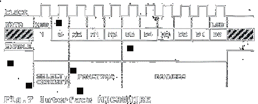 The GST Shifter ensures also the communication with circuit LMC1992 (controller hi-fi of volume and tonality) thanks to the signals *MWE, MWD, and MWK following to the Microwire Standard. These signals allow the configuration of the registers of the LMC1992. The data are serially transmitted by MWD (MicroWire Data) in synchronization with signal MWK (MicroWire clocK) provided that the signal *MWE (MicroWire Enable) is active (see figure 7). The message is on 11 bits: the 2 upper bits are always 1 and 0 to select the circuit, the 3 following bits are the circuit register number which corresponds to a command and the 6 lower bits are the data for the selected register.
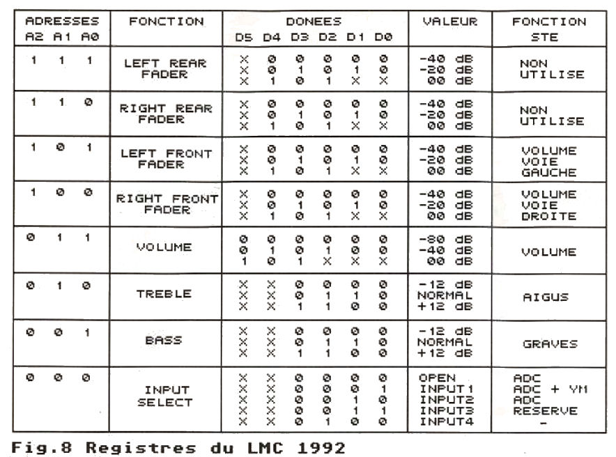
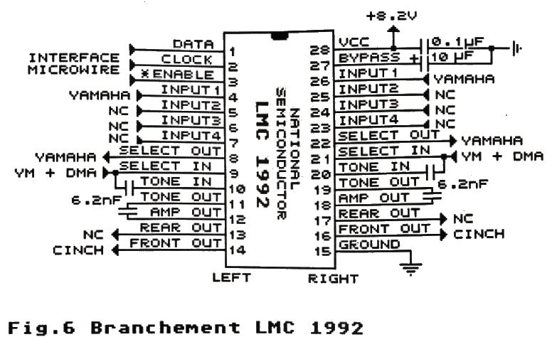 Figure 6 shows the pinout of the LMC1992 in the context of the STE. The distribution of the signals relative to the left and right channels is made on each sides of the package. The first three pins constitute the Microwire interface and are connected to the three corresponding signals of the Shifter. The circuit allows the selection by software of four stereo sources (input X), but only the first entry is used for the YM-2149 (see figure 5). This entry is selected by the system at starting time of the STE and if you select another entry (see registers of figure 8), the YM-2149 sound will not be heard anymore. Officially it is the entry 2 which must be selected to cut the sound of the YM-2149, whereas entry 3 is reserved (the entry 4 is not even mentioned!). Notice that the audio entry of the video connector is always there, even if it is not really useful. The LMC is planned for auto installations with four speakers, and therefore it has four exits (front and rear) of which only two are used (front) to go directly on the RCA connectors.
 Moreover, the two exits are reduced, mixed, and amplified to obtain a mono sound available on the video connector as on the STF. You can find the signal of the selected entry (YM-2149) on pins SELECT OUT. The signal is mixed with the output of MF004 filters, the result being amplified, then reinjected by SELECT IN pins. It is from there that the other registers (volume and tonality) act on the sound signal. Finally the filters carry out an anti-aliasing (removal of the staircases on the sound curve) with the assistance of a low pass filter whose frequency is 40% of that of sampling that is 2503, 5007, 10013, and 20026 Hz.
The response in tonality of the LMC is determined by the capacitors on the pins TONE IN and TONE OUT. But the bandwidth also varies according to these components with the default value of 0.0047 µF we have a bandwidth from 50 to 15.000 Hz. If we decrease the value to 0.0033 µF, the bandwidth becomes 70 to 20.000 Hz. For the STE it is the value of 0.0068 µF which is used, giving a bandwidth from 35 to 10.000 Hz. Add to that the remarkable quality of the sound treatment (amplifiers / filters) superior to the Amiga (limited to 28 Khz) and you can then hear the imperfections of the samples which however appear irreproachable on a STF (e.g. Quartet), proof of the much better bandwidth. All the registers relative to the sound DMA are given on figure 11. As for the video, some are not in the the GST Shifter but in GST MCU, namely: FBASE, FCOUNT, FEND, and PLAYMOD (not sure). Only SAMPMOD (not sure), LMCDATA and LMCMASK are in the Shifter.
Back to the topNew Joysticks / Paddles and Pen
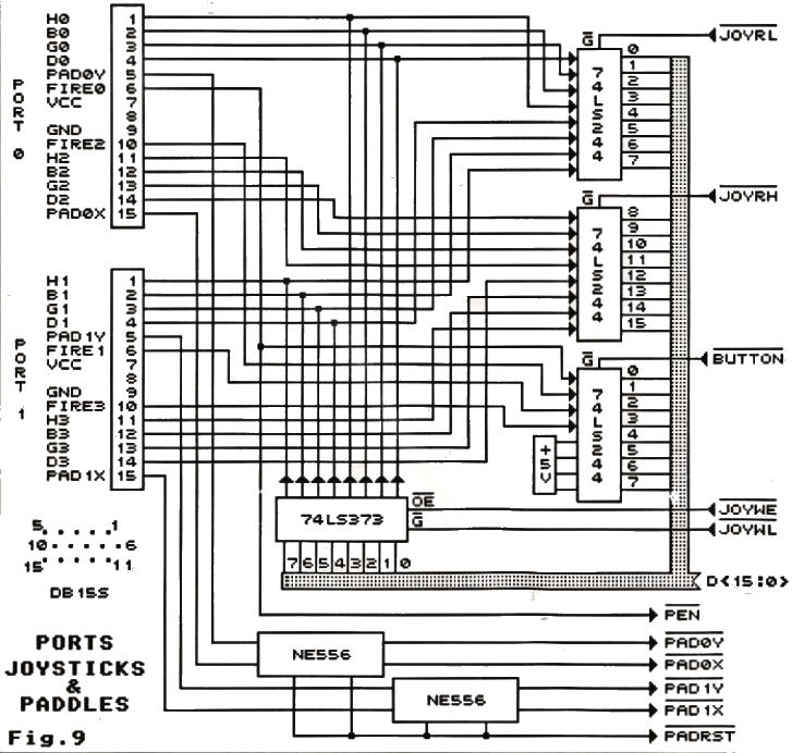 The third innovation of the STE is the addition on the left of two DB15 connectors making it possible to connect up to 4 joysticks, 2 paddles or 1 optical pen, but also the capability to drive external assemblies, because it is possible to write on these two ports. Figure 9 shows the connection diagram of these two ports to the system -- to simplify, the pull-up resistor networks were not represented.
On the right, one finds all the control signals which we had foreseen during the description of the GST MCU since it contains all the registers relative to the two ports (figure 12). The 4 bits of direction of the joysticks 0 and 1 are connected to the lower 8 bits of the data bus by a 74LS244 (hex buffer with 3 states) controlled by the signal *JOYRL (JOYsticks Read Low). In the same way, the 4 bits of the joysticks 2 and 3 are connected to the upper 8 bits of the bus controlled by the signal *JOYRH (JOYsticks Read High). Thus, only one 16 bits register contains the four directions of the four joysticks ($FF9202). A third 74LS244 activated by the signal *BUTTON, is used for the 4 bits FIREx, the 4 upper bits being always set to 1. Lastly, a 74LS373 (hex latch) makes it possible to send on the four pins of direction of the joysticks 0 and 1. respectively, the 4 lower bits and the 4 upper bits from the lower byte of the data bus. The capture of a byte (latch) is done with the reception of the signal *JOYWL (JOYstick Write Low) whereas the output of the circuit to toward the two ports is validated by the signal *JOYWE (JOYstick Write Enable). On each port, a paddle can be connected. This last informs of its position the GST MCU via a NE556 which contains two converters from voltage to pulses of variable frequency. In fact the the GST MCU analyzes the width of these impulses transmitted by the lines *PADxX and *PADxY and convert them to values from 0 to 255
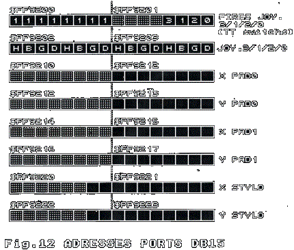 Lastly, it is possible to connect an optical pen, but I am not sure how! Two 10 bits registers should make it possible to read the position of the pen on the screen (10 bits to be able to encode the 640 points -- maximum for high-resolution) in X and Y. *PEN would be the signal sent to the GST MCU when one presses on the button of the pen. But it is not possible for me to say how the pen sends its position? I suppose that it uses the signals *PAD0X and *PAD0Y of the port 0.
Last remark: the register at the address $FF9200, that contains the 4 bits of the fire buttons, has another function. Indeed, the TOS 1.6 tests the bit 15 of this address. If you look on the board of the STE, close to the ROMs, you will see eight copper pastilles which act as switches that can be closed by soldering them. They are connected on one side to the ground and otherside to the 8 upper bits of the data bus via a 74LS244 validated by the signal *BUTTON applied at the time of an access in $FF9200. When there are no soldering points, as it is currently the case, the 74LS244 delivers 8 bits set to 1 thanks to a pull-up resistance network (+5v). You will be surprised to learn that in the TT, the address $FF9200 also exists and corresponds to 8 bits of system configuration (!), which proves that the TOS 1.6 is planned for the TT.
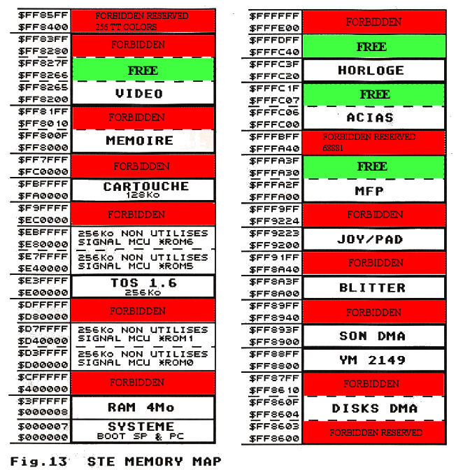
To finish, figure 13 represents the memory cartography of a STE, but from the hardware point of view. The GST MCU indicates an addressing error (two bombs) when an accesses to a "forbidden" zones is done. It exist several zones of free addresses which I particularly recommand for conceptors of addon boards. As for the zones "Forbidden - Reserved", they come from the Atari specifications; for example the zone FF8400-FF85FF accommodates the 256 color registers of the TT, whereas the zone FFFA40/FFFBFF is used by the 68881 coprocessor board referenced SFP004 for Mega ST.
This study of the hardware of the STE (and STF) are now finished, since the major points have been treated with the most details possible without going into too much technical considerations. I hope that it helps you to better understand this machine which has not yet finished to reveal its fantastic possibilities. Lastly, I make a point of sincerely thanking SIRIUS from ABCS85 for research in the ROMs and some system tests in assembler. OTARI for the document about the STE, BADMAN for the STE I exchanged against an Amiga, my mother for the food left in the freezer, Doudou for confidence that it carried me at the beginning of this project and my Mega ST which held good under extreme heat!
HardmaSTer ST Magazine N°44 September 1990
Back to the topAtari STE Related Documents
- STE Schematic Rev A
- STE TOS Release Note
- STE Developer Addendum
- STE Developer Information Addendum - From Markus Fritze site
- Atari STE FAQ compiled by The Paranoid / Paradox