This page contains information related to the Atari ST Floppy Disks from a "Hardware point of view". This includes information on the Floppy Disk Media, the FD Drives circuitry, electromagnetism, Disk encoding, FD Controller, etc ...
There is another page about the "Software side" of the ST Floppy disks containing information about FD layouts, Low and High level FD formatting, FD images, FD copy protection mechanisms, etc...
The information presented here should be useful for people designing programs for emulation, duplication (backup) or preservation (images) of Atari ST protected diskettes.
General Floppy Drives information
A lot of useful information about floppy drives and floppy disks can be found in this excellent documents: The floppy user guide by Michael Haardt, Alain Knaff, David C. Niemi. As well as in the document: The Technology of Magnetic Disk Storage by Steve Gibson. There is also this in depth document about disk drive technology
In this section we look at:
- Drive General Information
- Disk Storage basics
- Reading Data from the FD
- Writing Data to the FD
- Floppy Drive Read/Write Heads
- Sense, Amplification and Conversion Circuits
Drive Information
From the start, digital computers have required some form of data storage as an adjunct to their relatively sparse main storage facilities. Some of the early forms of storage were punched cards, paper tape and the magnetic tape storage. This was the principal storage medium, until faster-transfer, higher-capacity media became available and a direct link was established between the computer's main memory and the mass storage device. This link was the rotating memories, commonly referred to as disks.
The floppy disk consists of a thin sheet of Mylar plastic on which the gamma form of iron oxide is coated. The floppy disk is introduced in a disc drive that contains the head, and the control mechanism with its associated electronics. Each side of the disk consists of a number of thin annular regions called tracks. A double density 3-1/2 floppy disk usually contains 80 tracks. Each track is divided into blocks referred to as sectors. Data and other identification information are stored in the sectors. Floppy disc are soft sectored discs that have an index pulse signifying the start of a track. The reading or writing of data is accomplished by the read/write head. This head is positioned on the required track by the drives positioning control system. This process is commonly referred to as seeking. The rate at which data is written on the disk or read from it is termed as transfer rate. The speed at which a particular sector is found for the writing or reading of data is gauged by the access time. First the head must be positioned over the proper track referred to as seek time. Then the proper sector of the track must come under the head which is referred to as the latency time. Here is an example of specification about micro floppy drives: The Citizen X1DE-00R Micro Floppy Disk Drive Spec
Below is a functional block diagram of a SA800/801 8-inch floppy disc drive from Shugart.
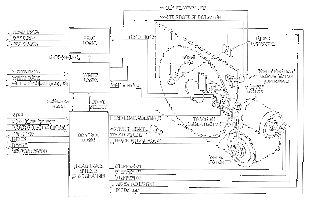
The block diagram for a typical 3 1⁄2-inch floppy disk drive would be very similar except that the index pulse is not detected by looking for an index hole. In 31/2” drive, the index sensor is not an optical sensor, as in the case of 5.25-inch drive. It uses the principle of Hall Effect. This disk gets locked in the drive, by a pin inside the drive getting into a dip near the center of the disk. At one side of the spindle motor, there is a magnetic material coating. As the spindle motor rotates, the sensor by the side of the spindle, gives out the pulses.
Back to the topFloppy Drive Read/Write Heads
The read/write heads on a floppy drive are used to convert binary data to electromagnetic pulses, when writing to the disk,
or the reverse, when reading. They are energy converters: they transform electrical signals to magnetic signals, and magnetic signals back to electrical
ones again. The read/write heads are in
essence tiny electromagnets that perform this conversion from electrical information to magnetic and back again. Each bit of data to be stored is
recorded onto the hard disk using a special encoding method that translates zeros and ones into patterns of magnetic flux reversals.
Conventional floppy disk ferrite heads work by making use of the two main principles of electromagnetic force. The
first is that applying an electrical current through a coil produces a magnetic field; this is used when writing to the disk. The direction of the magnetic
field produced depends on the direction that the current is flowing through the coil. The second is the opposite that applying a magnetic field to a coil will
cause an electrical current to flow; this is used when reading back the previously written information.
There are several important differences between floppy disk and hard disk read/write heads. One is that floppy disk heads are larger and much less precise than hard disk heads, because the track density of a floppy disk is much lower than that of a hard disk. The tracks are laid down with much less precision; in general, the technology is more "primitive". Hard disks have a track density of thousands of tracks per inch, while floppy disks have a track density of 135 tracks per inch or less.
In terms of technology, floppy disks still use the old ferrite style of head that was used on the oldest hard disks. In essence, this head is an iron core with wire wrapped around it to form a controllable electromagnet. The floppy drive, however, is a contact recording technology. This means that the heads directly contact the disk media, instead of using floating heads that skim over the surface the way hard disks do. Using direct contact results in more reliable data transfer with this more simplistic technology; it is impossible to maintain a consistent floating head gap at any rate when you are using flexible media like floppies. Since floppy disks spin at a much slower speed than hard disks--typically 300 to 360 RPM instead of the 3600 RPM or more of hard disks--they are able to contact the media without causing wear-out of the media's magnetic material. Over time, however, some wear does occur, and magnetic oxide and dirt builds up on the heads, which is why floppy disk heads must be periodically cleaned. Contact recording also makes the floppy disk system more sensitive to dirt-induced errors, caused by the media getting scratched or pitted. For this reason, floppy disks are much less reliable, overall, than hard disks.
The floppy disk also uses a special design that incorporates two erase heads in addition to the read/write head. These are called tunnel-erase heads. They are positioned behind and to each side of the read/write head. Their function is to erase any stray magnetic information that the read/write head might have recorded outside the defined track it is writing. They are necessary to keep each track on the floppy well-defined and separate from the others. Otherwise interference might result between the tracks. An alternate writing method to Tunnel Erasure is the Straddle Erasure: In this method, the R/W and the erasure heads do recording and erasing at the same time. The erasure head is not used to erase data stored in the diskette. It trims the top and bottom fringes of recorded flux reversals. The erasure heads reduce the effect of cross-talk between tracks and minimize the errors induced by minor run out problems on the diskette or diskette drive.
All modern--and even not-so-modern--floppy disks are double-sided. Very, very old floppy disks originally were single-sided only (early Atari 520 STF). Since the disks are double-sided, there are two heads, one per side, on the drive. The heads contact the media on each side by basically squeezing the media between them when the disk is inserted. The heads for different drives vary slightly based on the drive format and density used. Back to the top
Disk Storage Basics
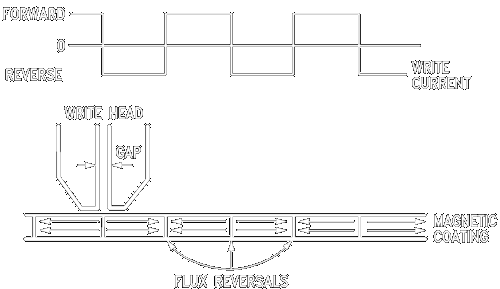 Magnetic writing the recording of data in a magnetic medium, is based on the principle that if a current flows in a coil of wire, it produces a magnetic field. The field is largely confined in a ring-shaped core of magnetic material, around which the wire is wound. A narrow slot is cut in the magnetic material and the field in the vicinity of the slot magnetizes the magnetic medium on the disk surface. Thus it creates alternating north-south magnets in the coated surface of the rotating disk. Thereby data is written.
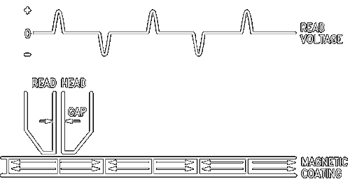 The head that writes the data can also be used to read it. This is done based on the principle of induction wherein a voltage is induced in an open circuit (like a loop of wire) by the presence of a changing magnetic field. In the case of a head positioned above a spinning magnetic disk on which data has been written, the magnetic fields emanate from the magnetized regions on the disk. During the time the head is over a single magnetized region, the field is more or less uniform. Hence no voltage develops across the coil that is part of the head. When a region passes under the head in which the magnetization of the medium reverses from one state to the other, i.e. a flux reversal, there is a rapid change in the field, developing a voltage pulse. In this way the digital data are read as an analog signal, which can be readily converted back to digital form.
The shape of this pulse and its ability to be recovered depends on various spacings. The core of most read/write heads is a ceramic consisting of spherical ferrite particles. The design of the head must conform to the design of the disk. In the case of the floppy disk, which is a thin sheet of mylar plastic on which the gamma form of iron oxide is coated, the head makes contact with the surface, resulting in higher error rates and greater wear of the medium (see section above).
Reading data from the disk
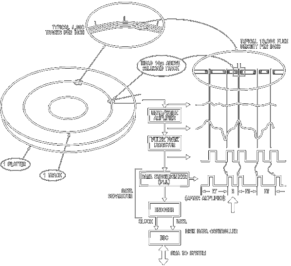 Reading data from the disk to the system memory is a complex process and involves a number of operations en-route, as shown in the following Figure. To initiate a read operation a command is sent to the disk drive indicating the track and sector from which data is to be read. The seek operation moves the head to the desired track on the disk. Eventually the desired sector is identified by the header ID segment and the various fields are checked depending on the formatting rules used. The flux reversals are recorded by the head. These pulses are then amplified by the read/write amplifier. The signal from the read/write amplifier when reading a disk is therefore a series of pulses with alternating polarity. These pulses are passed through a Pulse Detector. Electrically, these peaks correspond to flux reversals on the magnetic medium. The Disk Pulse Detector accurately replicates the time position of these peaks. The Disk Pulse Detector utilizes analog and digital circuitry to detect amplitude peaks of the signal received from the read/write amplifier associated with the heads of disk drives. A TTL compatible output is produced which on the positive leading edge indicates a signal peak. The raw data coming from the pulse detector consists of composite clock and data bits depending on the encoding scheme used. This encoded data has to be synchronized and decoded. These functions are performed by the Data Separator.
Data Separator
Due to bit shifting and distortion of the read pulses, the Pulse Detector issues non-synchronous pulses. For reliable decoding this jittery bit stream must be synchronized. The data separator has a Phase Locked Loop which attempts to lock on to the bit stream and synchronize it. For soft sectored drives, the controller normally will not wait for the Index pulse before it attempts lock-on. Chances are the head will not be over a preamble field and therefore there is no need to wait two bytes before attempting lock-on. Having locked-on to the bit stream the data synchronizer circuit must first determine the nominal position of clock and data bits and then generate an appropriate clock and data window that is centered around the bit positions. However there are many causes for bits to shift from the position where they are written. Erroneous data could be issued if bit jitter is beyond the tolerance computed. Therefore, special design considerations must be given to the type and resolution of the Data Separator used in reading data bits from the disk. The more accurately the bit position can be determined and the tighter the resolution of the data window, the lower is the soft error rate of the disk. Essentially the Data Separator's Phase Locked Loop locks on to the basic frequency of data bits read from the disk, and determines nominal bit positions for data and clock bits by sampling every bit (clock and data). It uses the phase relationship between a bit and its window to vary the position of the window. By sampling each bit, the phase-lock loop determines the phase error between a bit and the frequency being generated. To determine the nominal bit position around which to center the window, the data separator must track data bit frequency changes, yet ignore jitter. In this manner, even if an unpredictable bit shift occurs, the data separator can adjust the window's position to compensate for the change. Otherwise the shifted bit could be positioned outside the window. Once the bit stream read from the disk has been synchronized and decoded to NRZ data, it is directly sent to the Floppy Disk Controller block, FDC. In the FDC, the serial data is converted to parallel data (in terms of bytes), by the deserializer block. The main task is to recognize the byte boundaries accurately. In soft sectored drives this can be done by detecting a “missing clock” signal, which provides a fixed reference in the bit stream to set the byte boundary. Upon receipt of this signal the divide-by-eight circuit is set, to allow subsequent stages of the controller to acquire the bytes correctly. Once the data is in parallel form it is stored in a temporary register in the controller. Transfer of data from this register to the system memory is achieved by DMA (Direct Memory Access) transfer. In this fashion data are read from the disk and transferred to the system.
Back to the topWriting data to the disk
 The process of writing data to the disk is similar to the read operation in the reverse direction, with some changes. The write operation is initiated after the appropriate Seek command has been issued to the drive and the head is positioned over the desired track/sector. The following Figure shows the basic write path blocks.
Data is transferred from the system to the Controller using the DMA. The parallel data is converted to serial data by the serializer in the controller. This operation is conceptually easier to do, as the controller already has the right byte boundaries in the data and knows exactly where to insert the address mark. Most disk Controllers provide either NRZ encoded data or MFM encoded data. As mentioned in the previous section, predictable bit shift effects result from normal read/write head operation. Data are written when the read/write head generates a flux change in the media. In reading, a current is induced into the read/write head when a flux transition on the medium is encountered.
 The current change is not instantaneous, since it takes a finite time to build up to the peak and then to return to zero, refer to the figure on the right. If flux transitions are close together, the signal buildup after one flux transition declines, but it does not reach zero before a second transition begins. So when the flux changes are detected by the read/write head the peaks are shifted. A negative flux change, for example, may appear late because it has been added to the remnant of a positive transition. Narrower spacing between bits results in greater bit shift on the inner tracks.
Hence compensation is needed on the inner tracks to minimize bit shift while no compensation is required on the outer tracks as bit shift is negligible. Two methods being used are pre-compensation and post-compensation. With precompensation, bits are deliberately shifted in the direction opposite to that of the expected shift. As data are being written, the controller detects bit patterns. From these bit patterns, the controller calculates which bit will shift in which direction.
Sense, Amplification and Conversion Circuits
Since the signals read from the disk are very weak, special circuits are required to read the low-voltage signals coming from the drive heads, amplify them and interpret them, to decide if each signal read is a one or a zero. Information on magneto-dynamics and information comes from the SpinRight site. You may want to read this interesting document on the subject.
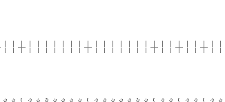
It is important to know that data pulses occurring near one another interact with one another. As previously explained, data bits are recorded on a magnetic surface by reversing the direction of the magnetism at a location. This magnetic reversal event is later picked up when the drive is reading. This event is treated as a data bit from the drive. Since a reversal of the magnetic field means making it go in the opposite direction, the signal picked up when reading the disk alternates in polarity, with a positive pulse followed by a negative pulse, followed by a positive pulse, followed by a negative pulse, and so on... If the pulses were ideal, perfect and square, the result would look something like this:
Notice that the pulses alternate in direction and return to the center.
But reality is much more messy. The diagram on the left shows a single, perfect, idealized pulse like those above, and the diagram on the right shows the actual shape of the pulse that is read back by a magnetic read head:
Ideal Pulse |
Actual Pulse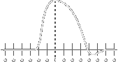 |
As you can see, the actual pulses are significantly rounded, are much broader, and even have a small overshoot near the end. This pulse breadth creates data pattern sensitivity because closely spaced pulses of opposite polarity overlap each other and partially cancel each other out.
Typical Worst Case Pulse Sequence:
In the diagram above, the first two pulses are spaced very far apart from all others so that they do not overlap and will be read as maximum amplitude pulses. This tricks the drive's read amplifier into turning down its amplification gain (Automatic Control Gain) since it presumes a strong signal coming from the drive's read head. But unlike the first two pulses, the last three pulses are spaced as closely together as possible. Lets look at what happens when we change our view from "theoretical pulses" to "actual pulses" ...
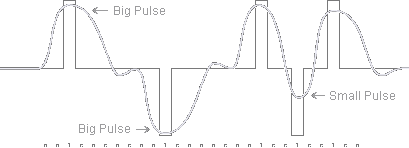
The big A and B pulses are read back with maximum amplitude because no other pulses are nearby. But the negative polarity D pulse, being tightly sandwiched in between the two positive polarity C and E pulses, gets pulled upward by its positive neighbors, so it isn't nearly as strong as it would normally be!
The first two isolated pulse set the drive's automatic gain control (ACG) to its minimum possible gain by creating maximum possible amplitude pulses. The next three pulses create a minimum-amplitude center pulse specifically designed to test the strength of the disk surface underneath the center pulse.
Back to the topNo Flux Area on Disk
There has been a lot of debate around the so called No Flux Area on disk. This is a protection's mechanism used on some floppies that results in absolutely no flux transitions coming from the data read circuitry.
Originally it has been thought that this was obtained by doing a "strong erasure" on some spots (sectors) of a disk. However this does not seems to be piratical to create. For one it cannot be done with the normal recording head/circuit of a floppy drive and therefore it would need to use a permanent magnet placed over the desired areas (again not really practical to do). Secondly if such no flux areas existed on the disk it would cause the ACG of the read chain to reach a maximum amplification and this would most probably result in random noise fluxes.
Therefore it is most likely that the following behavior is used to simulate no flux area on FD (note that this is what is actually used by some hardware copier like the Kryoflux board).
As you remember bit shift occurs on any NRZ recorded medium as a result from normal read/write head operation. Data are written when the read/write head generates a flux change in the gap of the head, which causes a change in magnetization of the medium oxide. In reading, a current is induced into the read/write head when a flux transition on the medium is encountered. The current change is not instantaneous, since it takes a finite time to build up to peak and then to return to zero. If flux transitions are close together, the current drop after one flux transition declines, but it does not reach zero before the second transition begins. When current pulses are summed by the read/write head, the peaks are shifted.
If you write fluxes close enough (obviously not respecting any encoding rules) this will result in having the current never returning to zero and therefore no data to be detected by the read channel. Note that the ACG is "happy" as the read chain receives flux transitions even if nothing is coming out.
Back to the topFloppy Disk Encoding/Decoding
Most of the information in this section are taken almost directly from Hard Disk Data Encoding / Decoding. You can also find interesting information about encoding in "RLL Technical Details" from Pete Holzman
Technical Requirements for Encoding and Decoding
You might think that since there are two magnetic polarities, N-S and S-N, they could be used nicely to represent a "one" and a "zero" respectively, to allow easy encoding of digital information. Simple! Well, that would be nice, but as with most things in real life, it doesn't work that way. There are three key reasons why it is not possible to do this simple 1-to-1 encoding:
- Fields vs. Reversals: Read/write heads are designed not to measure the actual polarity of the magnetic fields, but rather flux reversals, which occur when the head moves from an area that has north-south polarity to one that has south-north polarity, or vice-versa. The reason the heads are designed based on flux reversals instead of absolute magnetic field, is that reversals are easier to measure. When the disk head passes from over a reversal a small voltage spike is produced that can be picked up by the detection circuitry. As disk density increases, the strength of each individual magnetic field continues to decrease, which makes detection sensitivity critical. What this all means is that the encoding of data must be done based on flux reversals, and not the contents of the individual fields.
- Synchronization: Another consideration in the encoding of data is the necessity of using some sort of method of indicating where one bit ends and another begins. Even if we could use one polarity to represent a "one" and another to represent a "zero", what would happen if we needed to encode on the disk a stream of 1,000 consecutive zeros? It would be very difficult to tell where, say, bit 787 ended and bit 788 began. Imagine driving down a highway with no odometer or highway markings and being asked to stop exactly at mile #787 on the highway. It would be pretty hard to do, even if you knew where you started from and your exact speed.
- Field Separation: Although we can conceptually think of putting 1000 tiny N-S pole magnets in a row one after the other, in reality magnetic fields don't work this way. They are additive. Aligning 1000 small magnetic fields near each other would create one large magnetic field, 1000 times the size and strength of the individual components. Without getting too far into the details, let's just say that this would, in layman's terms, create a mess).
Therefore, in order to encode data on the hard disk so that we'll be able to read it back reliably, we need to take the issues above into account. We must encode using flux reversals, not absolute fields. We must keep the number of consecutive fields of same polarity to a minimum. And to keep track of which bit is where, some sort of clock synchronization must be added to the encoding sequence. Considering the highway example above, this is somewhat analogous to adding markers or milestones along the road.
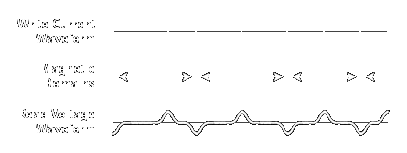 Idealized
depiction of the way hard disk data is written and then read.
The top waveform shows how patterns are written to the disk. In the
middle, a representation is shown of the way the media on the disk is
magnetized into domains of opposite direction based on the polarity of
the write current. The waveform on the bottom shows how the flux
transitions on the disk translate into positive and negative voltage
pulses when the disk is read. Note that the pattern above is made up
and doesn't follow any particular pattern or encoding method.
Idealized
depiction of the way hard disk data is written and then read.
The top waveform shows how patterns are written to the disk. In the
middle, a representation is shown of the way the media on the disk is
magnetized into domains of opposite direction based on the polarity of
the write current. The waveform on the bottom shows how the flux
transitions on the disk translate into positive and negative voltage
pulses when the disk is read. Note that the pattern above is made up
and doesn't follow any particular pattern or encoding method.
In addition to the requirements we just examined, there's another design limit that must be taken into account: the magnetization limits of the media itself. Each linear inch of space on a track can only store so many flux reversals. This is one of the limitations in recording density, the number of bits that can be stored on the platter surface. Since we need to use some flux reversals to provide clock synchronization, these are not available for data. A prime goal of data encoding methods is therefore to decrease the number of flux reversals used for clocking relative to the number used for real data.
The earliest encoding methods were relatively primitive and wasted a lot of flux reversals on clock information. Over time, storage engineers discovered progressively better methods that used fewer flux reversals to encode the same amount of information. This allowed the data to effectively be packed tighter into the same amount of space. It's important to understand the distinction of what density means in this context. Hardware technology strives to allow more bits to be stored in the same area by allowing more flux reversals per linear inch of track. Encoding methods strive to allow more bits to be stored by allowing more bits to be encoded (on average) per flux reversal.
Back to the topFrequency Modulation (FM)
The first common encoding system for recording digital data on magnetic media was frequency modulation, of course abbreviated FM. This is a simple scheme, where a one is recorded as two consecutive flux reversals, and a zero is recorded as a flux reversal followed by no flux reversal. This can also be thought of as follows: a flux reversal is made at the start of each bit to represent the clock, and then an additional reversal is added in the middle of each bit for a one, while the additional reversal is omitted for a zero.
This table shows the encoding pattern for FM (where I have designated "R" to represent a flux reversal and "N" to represent no flux reversal). The average number of flux reversals per bit on a random bit stream pattern is 1.5. The best case (all zeroes) would be 1, the worst case (all ones) would be 2:
Bit Pattern |
Encoding Pattern |
Flux Reversals Per Bit |
Bit Pattern Commonality In Random Bit Stream |
0 |
RN |
1 |
50% |
1 |
RR |
2 |
50% |
Weighted Average |
1.5 |
100% |
|
The name "frequency modulation" comes from the fact that the number of reversals is doubled for ones compared to that for zeros. This can be seen in the patterns that are created if you look at the encoding pattern of a stream of ones or zeros. A byte of zeroes would be encoded as "RNRNRNRNRNRNRNRN", while a byte of all ones would be "RRRRRRRRRRRRRRRR". As you can see, the ones have double the frequency of reversals compared to the zeros; hence frequency modulation (meaning, changing frequency based on data value).
 |
| FM encoding write waveform for the byte "10001111". Each bit cell is depicted as a blue rectangle with a pink line representing the position where a reversal is placed, if necessary, in the middle of the cell. |
The problem with FM is that it is very wasteful: each bit requires two flux reversal positions, with a flux reversal being added for clocking every bit. Compared to more advanced encoding methods that try to reduce the number of clocking reversals, FM requires double (or more) the number of reversals for the same amount of data. This method was used on the earliest floppy disk drives, the immediate ancestors of those used in PCs. If you remember using "single density" floppy disks in the late 1970s or early 1980s, that designation commonly refers to magnetic storage using FM encoding. FM was actually made obsolete by MFM before the IBM PC was introduced, but it provides the basis for understanding MFM
Back to the topModified Frequency Modulation (MFM)
A refinement of the FM encoding method is modified frequency modulation, or MFM. MFM improves on FM by reducing the number of flux reversals inserted just for the clock. Instead of inserting a clock reversal at the start of every bit, one is inserted only between consecutive zeros. When a 1 is involved there is already a reversal (in the middle of the bit) so additional clocking reversals are not needed. When a zero is preceded by a 1, we similarly know there was recently a reversal and another is not needed. Only long strings of zeros have to be "broken up" by adding clocking reversals.
This table shows the encoding pattern for MFM (where I have designated "R" to represent a flux reversal and "N" to represent no flux reversal). The average number of flux reversals per bit on a random bit stream pattern is 0.75. The best case (a repeating pattern of ones and zeros, "101010...") would be 0.25, the worst case (all ones or all zeros) would be 1:
Bit Pattern |
Encoding Pattern |
Flux Reversals Per Bit |
Bit Pattern Commonality In Random Bit Stream |
0 (preceded by 0) |
RN |
1 |
25% |
0 (preceded by 1) |
NN |
0 |
25% |
1 |
NR |
1 |
50% |
Weighted Average |
0.75 |
100% |
|
Since the average number of reversals per bit is half that of FM, the clock frequency of the encoding pattern can be doubled, allowing for approximately double the storage capacity of FM for the same area density. The only cost is somewhat increased complexity in the encoding and decoding circuits, since the algorithm is a bit more complicated. However, this isn't a big deal for controller designers, and is a small price to pay for.
|
| FM and MFM encoding write waveform for the byte "10001111". As you can see, MFM encodes the same data in half as much space, by using half as many flux reversals per bit of data. |
Since the MFM method about doubles the capacity of floppy disks compared to earlier FM ones, these disks were called "double density". In fact, MFM is still the standard that is used for floppy disks today. For hard disks it was replaced by the more efficient RLL methods. This did not happen for floppy disks, presumably because the need for more efficiency was not nearly so great, compared to the need for backward compatibility with existing media. Note that MFM encoding is sometimes called 1,3 RLL as the pauses run length, between pulse, are in the range 1 to 3 (see RLL Technical Details).
Western Digital WD1772 Information
This section contain few information about the inner working of WD1772 Floppy Disc Controller used in Atari ST machines. More specifically we will be looking at the following blocks in the FDC
For more more information read the Western Digital datasheet. Also of interest is the programming information document as well as an interesting article on FDC from David Small.
Sub-sections:
- WD1772 PLL Data Separator
- Detail on Inspection Window
- Detection of Fuzzy bits by the WD1772
- FDC Address Mark Detector
- FDC CRC
WD1772 DPLL Data Separator
As shown in the above diagram the WD1772 floppy disc controller has an internal DPLL data separator unit used to separate the clock bits from the data bits. This data separator is locked onto the incoming serial data and must still work for a certain amount of frequency variation on the input. When locking is achieved the front end logic of the chip is provided with a clock synchronized to the read data. This synchronized clock, called Inspection Window, is used to internally sample the serial data. One state of the Inspection Window is used to sample the data bit of a cell, and the alternate state samples the clock bit. Serial to parallel conversion logic separates the read data into clock and data bytes and feed them into the DSR (Data Shift Register).
To support reliable disk reads the data separator must track fluctuations in the read data frequency. Frequency errors primarily arise from two sources: motor rotation speed variation (MSV) and instantaneous speed variation (ISV). Note that a second condition, and one that opposes the ability to track frequency shifts is the response to bit jitter.
- Jitter tolerance definition: The jitter immunity of the system is dominated by the data PLL's response to phase impulses. This is measured as a percentage of the theoretical inspection window by dividing the maximum readable bit shift by a 1/4 bit-cell distance.
- Locktime definition: The lock, or settling time of the data PLL is usually designed to be 64-bit times (8 sync bytes). The value assumes that the sync field jitter is 5% the bit cell or less. This level of jitter is realistic for a constant bit pattern. Inter symbol interference should be equal, thus nearly eliminating random bit shifting.
- Capture range definition: Capture Range is the maximum frequency range over which the data separator will acquire phase lock with the incoming data signal. In a floppy disk environment, this frequency variation is composed of two components: drive motor speed error and ISV (Instantaneous Speed Variation). Frequency is a factor which may determine the maximum level of the ISV component. In general, as frequency increases the allowed magnitude of the ISV component will decrease.
Unfortunately detailed information on the 3 important PLL parameters: jitter tolerance, locktime, and capture range is NOT provided in the WD1772 documentation.
Note that the IBM standard allow deviation of the rotation speed of the drive within less than 2% range and therefore the PLL in the FDC is supposed to tolerate a 4% variation from central frequency. In practice the PLL of the WD1772 will cope with at least 10% variation for MFM encoding and 100% variation for FM encoding. It is therefore possible to write bit cell at a frequency between 225 to 275 KHz (i.e. 3.4µs to 4.4µs cell width) in MFM and still be able to read these bits correctly.
For general information on PLL there is an excellent, and easy to understand, document on Phase-Locked Loops subject: A Control Centric Tutorial by Danny Abramovitch. Look also at Phase lock loop with application document.
However if you want to understand the kind of DPLL separator used in the WD1772 you should look at the following patents
- US Patent 4357707 - Digital Phase Lock Loop for Flexible Disk Data Recovery System
- US Patent 4780844 - Data Input Circuit with Digital Phase Lock Loop
- US Patent 4808884 - High Order Digital Phase-Locked Loop System
- US Patent 5592515 - Fully Digital Data Separator and Frequency Multiplier
It is not possible to know if any of these patents describe the DPLL of the WD1772. Below we base our analysis on patent US 4780844 which describe clearly the work of a DPLL and data separator. In this patent the Inspection windows are established that have duration proportional to the frequency of arrival of the data, and start/stop times that can be adjusted so that subsequent data bits will be received in the middle of the inspection windows. To achieve this, the DPLL circuitry applies frequency and phase corrections that compensate the input data frequency drift. This drifts are usually due to unsteadiness of the motor drive speed (the frequency drift), and the migrations of the magnetic reversals area (the phase drift).
Back to the topDetail on the Inspection Window
As we have seen the WD1772 uses a digital phase lock loop (DPLL) circuit for reading the input data transmitted from FD media. Inspection windows are established that have duration proportional to the frequency of arrival of the data, and start/stop times that can be adjusted so that subsequent data bits will be received in the middle of the inspection windows. To achieve this, the DPLL circuitry applies frequency and phase corrections that compensate the input data frequency drift. This drifts are usually due to unsteadiness of the motor drive speed (the frequency drift), and the migrations of the magnetic transition area (the phase drift). The DPLL used inside the WD1772, as well as many other FDC build in the 80s, probably implements the algorithm described in the public US patent 4,870,844. The patent is rather complex and in this section I will only highlight some of the most important aspects of the DPLL algorithm that are useful to understand the behavior in the context of fuzzy bits, long/short track, etc.
Let’s first look at typical MFM data encoding:
As we can see the nominal values for the possible transitions spacing in DD MFM (1MB mode) are: 4µs, 6µs, or 8µs.
The data input circuit of the FDC ensures that the data pulses received are converted into data bits and stored in the data shift register (DSR). For that matter the digital phase lock loop defines inspection windows that repeat every 2µs (a half cell size). A one is input to the shift register if a data pulse is received at any time during one inspection windows; otherwise a zero is stored in the shift register as the value for the current bit.
The period of the inspection windows is gradually adjusted (expanded or shortened) to compensate an eventual frequency shift affecting the input data transfer. This frequency correction is computed based on the history of the location (relative to the inspection window) of the last three flux transitions.
 Ideally, individual pulses should be located in the middle of the inspection windows. To achieve this, the start and stop times of the inspection windows are adjusted to compensate for deviation (from ideal) in time of arrival of the most recently detected data pulse. This phase correction is done proportionally to the distance of the transition with the middle of the inspection window.
The proper ratio of phase and frequency correction provided in the loop is carefully balanced so that the DPLL is fast settling but stable. A large amount of phase correction cause the loop to settle faster but also make it more sensible to noise. On the other hand if too much frequency correction is used, the loop can become unstable. It is interesting to note that the DPLL as defined in the patent allow an input frequency variation of up to 9%. This corroborates the actual measurement made with a WD1772 that correctly interprets bits with a variation of at least 9 to 10 % for DD MFM (and about 100% for SD FM!). Note that these values are well above the variation used by the Copylock and Macrodos protection mechanisms (usually less than 5%) and therefore the data within this kind of sector should be read correctly.
Detection of Fuzzy "Border" Bits by the WD1772
There are several ways to create Fuzzy bits. Here we will described the creation/detection of fuzzy bits by placing flux reversal at the border of the inspection window. This is used by the Game Dungeon Master and it is described in the patent Copy Protection for computer Disc 4,849,836.
With the above information about the inspection window it is now easy to understand that if a flux transition happens close to the border of an inspection window (aka uncertain area) it will be detected into the first or the next inspection window based on small variation of the drive rotation speed between read-sector commands and this will therefore result in pseudo random values returned (fuzzy bits).
For example having a transition 5µs apart from the previous one can be interpreted as a transition after 4µs or a transition after 6µs based on small frequency fluctuation of the rotation speed between two reads. One might argue that it is not possible to make sure that these “marginal transitions” will be positioned correctly due to the fact that the rotation’s speeds of different drives are somewhat different and therefore precise transition timing on a floppy diskette cannot be guaranteed. But in practice this is where the frequency and phase correction of the WD1772 DPLL comes into play. As explained above the inspection window will have it size (i.e. frequency) and position corrected based on the input transition stream after reception of only a few transitions. Therefore the DPLL of the FDC automatically adjust the frequency of inspection windows for any acceptable (about 10%) variation of drive speed and adjust the phase so that a “normal transitions” will be perfectly in the middle of the inspection window and a “marginal transition” will be perfectly at the border of the inspection window.
This also explains why, in most cases, “fuzzy bits” are used in “compensating pair”: for every two subsequent fuzzy bits the first transition is placed at one extreme (e.g. at the beginning) of the inspection window and the “compensating transition” of the next fuzzy bit at the other extreme (e.g. at the end) of the inspection window. By using this kind of “compensating bits” we guarantee that the frequency and the phase of the inspection windows are (almost) not affected.
FDC Address Mark Detector
The purpose of the Address Mark Detector in the FDC is to be able to recognize an address mark in the flow of data received from the floppy drive. For that matter we also need a non-ambiguous way to find the start of a byte in the flow of bits (data synchronization).
FM Address Marks
In FM encoding (not used by the Atari ST) synchronization is done by looking for an Address Mark with missing clock (normal bytes use an FF clock pattern)
| ADDRESS MARK | Data Pattern | Clock Pattern |
| Index Address Mark | FC | D7 |
| ID Address Mark | FE | C7 |
| Data Address Mark | FB | C7 |
| Deleted Data Address Mark | F8 | C7 |
MFM Address Marks
As we have already explained with MFM encoding a clock is only added for two consecutive 0 data bits and it is therefore not possible to differentiate between clock and data bits on arbitrary sequence of bits.
In MFM encoding (used by the Atari ST) synchronization is done by searching for a sequence of special bytes.
- First, there is a special data sequence encoded at the beginning of each ID and DATA field: a long string of zero's. This sequence provides to the DPLL enough time to adjust the frequency and center the inspection window. This is especially important for the DATA field because a Write splice occurs when the read/ write head starts re-writing a data field. The slight variations in the rotational speeds cause the first flux change to occur in different positions for each write operation and therefore the DPLL needs to adjust to this new frequency/position.
- Second, special bytes are encoded that violates the MFM encoding rules: either $A1 or $C2 bytes are written, with a missing clock in one of the sequential zero bits. These 2 special bytes with missing clocks are called the Sync Bytes. In practice there is a sequence of 3 consecutive Sync Bytes that should normally be followed by an Address Mark (IAM, IDAM, or DAM) as described in the track format.
In summary if a sequence of zeros followed by a sequence of three Sync Bytes is found, then the PLL (phase locked loop) and data separator are synchronized and data bytes can be read. The following table shows the Sync Bytes and the Address marks used by the WD1772 on the Atari ST
| ADDRESS MARK | Data Pattern | Clock Pattern | Missing clock between bits (1) | Resulting Bit Sequence |
| Sync Byte (before IDAM or DAM) | $A1 | $0A | 4 &5 | 0100010010001001 ($4489) |
| Sync Byte (before IAM) | $C2 | $14 | 3 & 4 | 0101001000100100 ($5224) |
| Index Address Mark (IAM) | $FC | |||
| ID Address Mark (IDAM) | $FE | |||
| Data Address Mark (DAM) | $FB | |||
| Deleted Data Address Mark (DDAM) | $F8 |
(1) The bits order is from MSB to LSB (the way they are sent) with first bit being numbered 0 (Thanks to Ijor for clarification). Note that this encoding does not violate the 1,3 RLL rules (sequence of 4 consecutive 0) and therefore it is possible to find in a stream some bit configuration that are the same as the $C2 synch mark. This is known as the false sync byte pattern problem/bug during a read track command.
Note that with the WD1772 an $A1 sync byte is produced by sending a $F5 byte to the FDC during the command, a $C2 sync byte is produced by sending a $F6 byte, and that the 2 bytes CRC are written by sending one $F7 byte. Normally the $C2 sync byte is is only used before an IAM and therefore normally not used in standard Atari diskettes. However having an IAM records on a track (as formatted on a PC) is perfectly acceptable on an Atari.
Back to the topMFM Synch Byte Pattern
Figures below depict the $A1 and $C2 bytes with and without missing clock (for simplicity the following representation depicts the flux reversal as ideal pulses):
|
|
| $A1 with missing clock | Normal $A1 |
 |
 |
| $C2 with missing clock | Normal $C2 |

False Synch Byte Pattern
During normal reading of a data sector the Sync Mark Detector of the WD1772
is disabled. However during a read track command the
sync mark detector is active all the time. It has been said that the WD1772 has a bug that causes it to mistakenly find $C2 sync mark inside data
(for example see "copy
me I want to travel" from Claus Brod). Well in
fact I find that the Sync Mark Detector does it job perfectly! it is just that the $C2 sync mark has not
been chosen wisely. For that reason it is quite possible to
find several sequences of bits (see
what Gunstick says on the subject) that have the exact same pattern as
the $C2 with missing clock!
The consequence is that if you have a sequence of
bits that matches the $C2 sync byte inside a data block and if you read it with
a read track command then the FDC
synchronizes on this pattern and the following bits are shifted resulting in a totally different
reading of this sector! This "feature" can be used
as a protection mechanism to hide some information
inside a data block (read my protection document).
For example if we encode the $x029 sequence we get the following result:
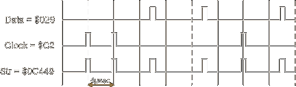
And as you can see we can find the sync byte $C2 with missing clock in this sequence of bits (shifted by a half cell) !
Note that there are many known sequences that matches the $C2 sync byte, but I have not been able to find any sequence that matches the $A1 sync byte (does not mean that it does not exist!).
Back to the topFDC CRC
Computing CRC in hardware
The CRC generator used by the FDC uses the classical CCITT polynomial G(x)=x^16 + x^12 + x^5 + 1.
Typically, CRC calculations are implemented with linear-feedback shift registers (LFSRs). LFSRs use a method that yields the same results as the subtract and shift division process when the subtraction is performed
without carry by the XOR function. To affect the subtract and shift division one bit at a time, you can shift through and examine each bit in the original frame of data (for example, the dividend). For the first bit of value 1, the divisor high-order bit is subtracted (XORed) from the dividend. That dividend bit, which is unnecessary and is not generated, is set to zero by the subtraction. The lower order bits of the divisor cannot
be subtracted yet, because the corresponding divisor bits have not been shifted in.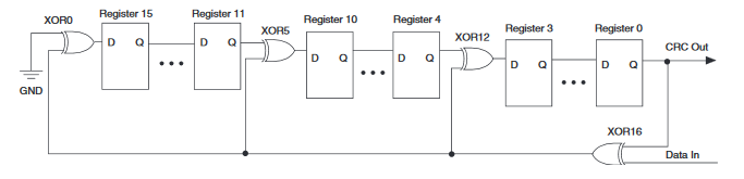
The figure shows the Consultative Committee International Telegraph and Telephone (CCITT) CRC-16 generator computed serially. The quotient “1” bit (XOR16) is fed back and subtracted from the appropriate taps in the shift register (XOR12, XOR5, XOR0). These bits shift forward to appear at the end and are subtracted from the next data bit, unless they are eliminated by a coinciding second bit from an earlier or later subtraction that is fed back.
The CRC figure originally posted on this page was wrong. Thanks to Eric H. that have pointed me to the correct figure.
At the beginning, all flip flops of the register are set to 1 (initialized to $FFFF). After the last data bit is processed, the register contains the CRC. For checking CRC, you do the same, but the last you feed to it is the CRC. If all is fine, then all bits will be 0 after. Since bytes are recorded with their highest bit first on floppies, they are also processed by the CRC register that way and the resulting CRC will be written with bit 15 being the first and bit 0 being the last to the floppy (big Indian). The CRC is processed beginning with the first $A1 byte which presets the CRC register, so the CRC of a typical ID record would be computed for example as CRC of " $A1, $A1, $A1, $FE, $00, $00, $03, $02" and have the value $AC0D. Where $AC will be the first CRC byte and $0D the second.
In summary the 16 bit CRC of the WD1772 is generated using the CCITT generator polynomial. It is initialized to $FFFF and the computation includes all characters starting with the first $A1 until the last CRC character. It is recorded and read most significant bit first.
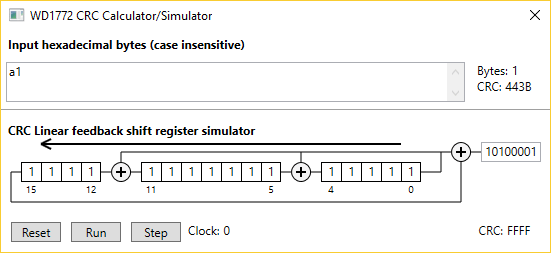 I have written a small Windows WPF program that computes the CRC of a string of hexadecimal characters. It is also possible to displays a simulation of the CRC computation in hardware. The figure on the right shows the usage of this program on a single A1 string.
You can download this program here.
Usage:
- Enter a string of hexadecimal characters in the input window and the CRC is immediately computed (every two characters).
- To run the LFSR simulator you need first to click the RESET button after you have entered the input string.
- Click the RUN button to animate the LFSR until all character are processed.
- Click the STEP button to shift one bit at a time in the simulator.
Note-1: The WD1772 documentation is somewhat ambiguous on the subject of CRC
computation. It is mentioned that, in MFM, the CRC is initialized by receipt of $F5
byte but the value used for initialization is not indicated. I have verified that if you initialize the CRC to $FFFF (all one as described page 1-3 of the documentation) on the first $A1 and just treat the next two $A1 as normal bytes then the CRC is computed correctly. But another possibility proposed by Ijor is to initialize the CRC to $C4DB each time a $A1 is received. I you are writing an emulator both solution should work correctly on a standard sequence of 3 $A1 in front of an AM.
Note-2: It is also possible to use $C2 as a sync byte, but in this case
beware that the CRC
is not reset. Therefore writing a sequence like " $C2,
$C2, $C2 $FE $00 $00 $03 $02 " is read correctly by the FDC but it results in a wrong CRC
(this is often used for protection read my protection document).
Computing CRC in software
There are many articles and examples of CCITT-CRC code available on the net. I have selected this one in French Le contrôle CRC by Julien Rosener and these ones in English A painless guide to crc error detection algorithm and crctable.c by Ross Williams, crcccitt.c - a demonstration of look up table based CRC by Jack Klein, ...
But the code I prefer was exposed here by Simon Owen in the Atari forum:
"The basic code to compute the CRC is"
for (int i = 0; i < 8; i++) crc = (crc << 1) ^ ((((crc >> 8) ^ (b << i)) & 0x0080) ? 0x1021 : 0);
"Or use a normal CRC-CCITT look-up table for much faster computation:"
crc = (crc << 8) ^ crc_ccitt[((crc >> 8) & 0xff) ^ b];"Where the look-up table is the normal one generated from the 0x1021 polynomial using something like: "
for (int i = 0; i < 256; i++) { WORD w = i << 8; for (int j = 0; j < 8; j++) w = (w << 1) ^ ((w & 0x8000) ? 0x1021 : 0); crc_ccitt[i] = w; }
You can find here a small test program (with sources), I have developed based
on the above code. The program only runs on a PC
Thanks to Steve C. that found an error (now corrected) in the code using a lookup table ![]()
Documents & Links
Floppy Disk, Magnetic recording interesting documents
- Disk Interface Design Guide and User's Manual - NS AN413
- Precaution for Disk Data Separator PLL Designs - NS AN414
- Floppy Disk Data Separator Design Guide for the DP8473 - NS AN505
- Reading and Writing in Floppy Disk Systems using Motorola IC - Motorola AN917
- FDC 9216 Floppy Disk Data Separator - SMC TN6-1
- Encoding Decoding Techniques Double FD Capacity J.F. Hoeppner and L.H. Wall - Shugart Associates
- Patent US 4357707 - Digital Phase Lock Loop for Flexible Disk Data Recovery System
- Patent US 4780844 - Data Input Circuit with Digital Phase Lock Loop
- Patent US 4808884 - High Order Digital Phase-Locked Loop System
- Patent US 5592515 - Fully Digital Data Separator and Frequency Multiplier
- Patent US 7983370 B2 - Clock and Data Recovery Circuit
- Patent US 4849836 - Copy Protection for Computer Discs (Dungeon Master & CSB)
- Magnetic Recording Fundamental
- Magnetic Materials - Recording
- Floppies: controllers, cabinets, disks, docs & hints from retrotechnology
- Tech information on floppy disks drives and media from retrotechnology
- Floppy Disk from Wikipedia
- Floppy Disk Drives from PC Guide
- How Floppy Disk Drives Work
- The Floppy User Guide - M. Haardt, A. Knaff, D.C. Niemi
- The Technology of Magnetic Disk Storage by Steve Gibson
- Floppy Primer
- Cours de Periphériques - Lecteur de disquettes (in French)
- copy me I want to travel
- A Method for Recovering Data from Failing FD Drives Dr. F.B. Cohen and C. Preston
- SpinRite's Defect Detection Magnetodynamics Magnetic Storage Rocket Science)
- Fundamental Audio production - Recording ....
- Digital Magnetic Tape Recording Fundamental - Training Material
Drive Documents
- SF354 Users Manual
- SF354 Service Manual
- The floppy user guide
- The Technology of Magnetic Disk Storage
- The Citizen X1DE-00R Micro Floppy Disk Drive Spec
Floppy Disk Controllers
- Western Digital 177X-00 or better version from DrCoolZic
- Texas TMS 279X (equivalent from Texas)
- Western Digital WD279X-02
- Western Digital FD1771
- Intel 8271
- Intel 8272
CRC
- CRC computation in C by obo (Simon Owen)
- A painless guide to crc error detection algorithm
- crctable.c by Ross Williams
- Tutoriel sur le calcul des CRC
- Le contrôle CRC by Julien Rosener
- crcccitt.c - a demonstration of look up table based CRC by Jack Klein
- The cyclic Redundancy Check for AX.25
- CRC16-CCITT
- CRC (Wikipedia)
- Computation of cyclic redundancy checks
- Implementing CRC in Altera Devices